Why?
While we already have instruction level parallelism, some loop iterations and other code can benefit from parallel computation. The most obvious example is graphics processing in GPUs. Often-times, these computations are (or can be thought of as) a vector that is multiplied by a scalar or other vector.
Necessary Architectural Resources
Vector registers: each holds a vector of maximum length (max vector length)
Vector functional units: Fully pipelined, II = 1 cycle
Vector Load/Store Unit: Fully pipelined
Predicate registers: to support conditional execution
Optimization: Dynamic Register Configuration: Allows flexible trading of between number of vectors, width of vector elements, and .
- E.g. 1 KiB of vector register space, configure as 4 VRs of doubles, each VR gets 256 B, so
Can disable VRs under program control, reducing program state that needs to be saved on context switches.
Modeling Execution Time
We can model the execution time as a function of three factors:
- Length of operand vectors
- Data dependences
- Structural hazards (trying to put more data through than is possible)
Assume that in this example the Functional Unit processes one element per clock cycle.
We can handle read-after-write (RAW) dependences by chaining: essentially a pipelined version of forwarding that allows a dependent vector operation to start as soon as individual elements of its vector source operand become available.
We can group vector instructions into different convoys
- A convoy is a set of vector instructions that have no structural hazards and could therefore potentially execute together
- A chime is the unit of time to execute one convoy
The model is:
- Time for one chime vector length (proportional)
- Total time number of convoys
- For convoys and vectors of length , the total time is clock cycles
Example
Assume the following code:
L1: V0 <- (X5) # Vector Load
L2: V1 <- V0 * F0 # Vector * Scalar
L3: V2 <- (X6) # Vector Load
L4: V3 <- V1 + V2 # Vector + Vector
L5: (X6) <- V3 # Vector Store
We have 3 convoys:
L1, L2L3, L4L5
For vectors of length 32, the model gives an execution time of clock cycles. This analysis ignores the pipeline startup times. Suppose FPADD has a latency of 6 cycles, FPMUL 7, and FPLD 12.
The timing ends up looking like this:
| Instruction | Init | FRes | LRes |
|---|---|---|---|
| L1 | 0 | 12 | 43 |
| L2 | 13 | 20 | 51 |
| L3 | 43 | 55 | 86 |
| L4 | 56 | 62 | 93 |
| L5 | 86 | > 118 |
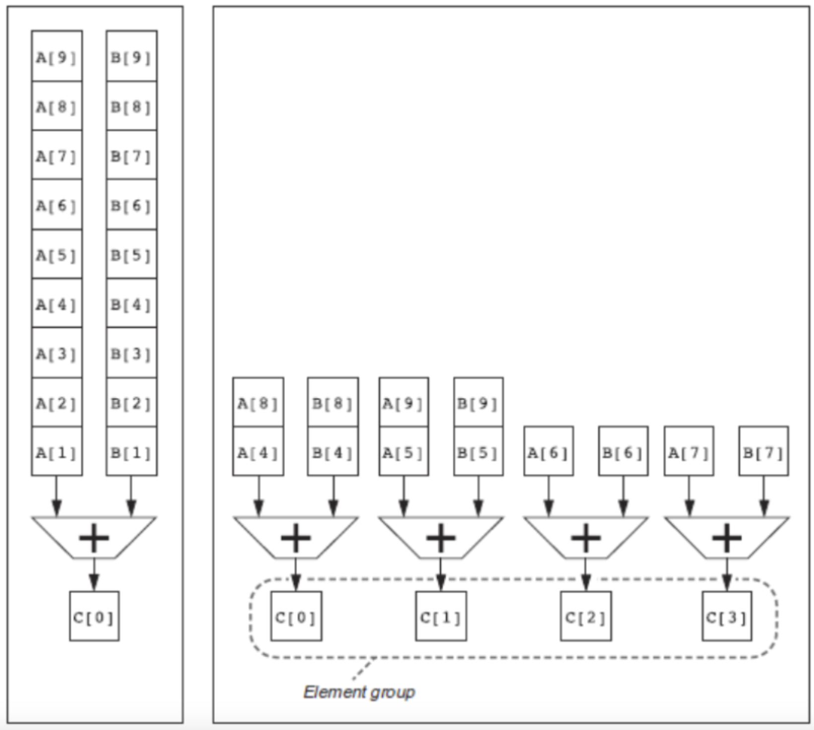
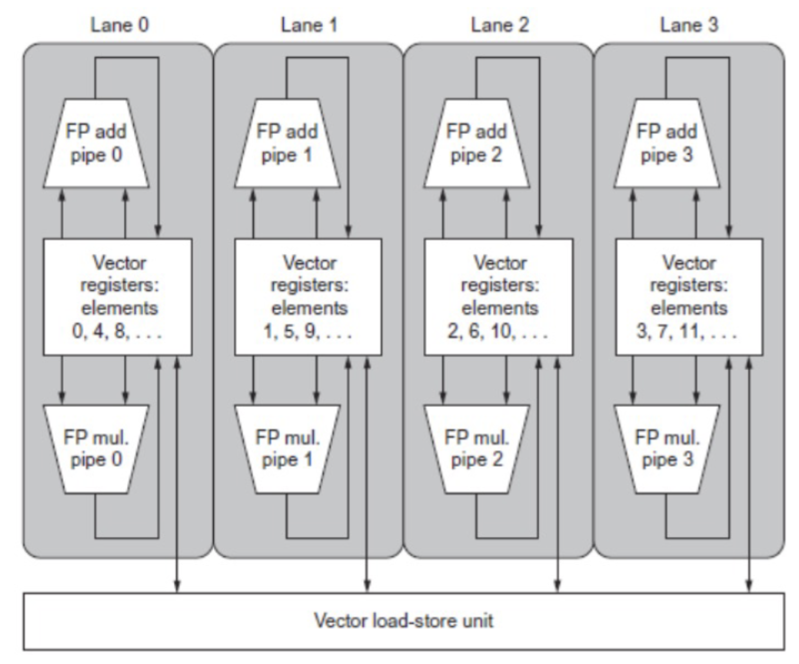
Architectural Enhancements
Multiple hardware lanes
 |  |
|---|
Vector Mask Registers (aka Predicate Registers)
Consider the code:
for (i = 0; i < 64; i++)
	if (X[i] != 0)
		X[i] = X[i] - Y[i];
Using predicate registers to “disable” elements:
vsetdcfg 2*FP64 # Enable 64b FP Vector Registers
vseetpcfgi 1 # Enable 1 Predicate Register
vid v0, x5 # Load Vector X into V0
vid v1, x6 # Load Vector Y into V1
fmv.d.x f1, x0 # Put (FP) Zero into F0
vpne p0, v0, f0 # Set P0(i) to 1 if V0(i) != F0
vsub v0, v0 v1 # Subtract under Vector Mask
vst v0, x5 # Store result in X
vdisable # Disable vector registers
vpdisable # Disable Predicate Registers
Highly Interleaved Memory Subsystem
In a processor with vector calculations, the memory bus needs to support a ton of memory going across. As a result, it has to have a beefed up memory system. It must be designed specifically to support high bandwidth for vector loads and stores.
The best way to do this is to spread accesses across multiple banks so we have parallelism within the memory subsystem itself: control bank addresses independently, load or store non-sequential words, support multiple vector processors sharing the same memory.
Example
32 processors, each generating 4 loads and 2 stores/cycle =
The processor cycle time is 2.167ns, the SRAM cycle time is 15ns
If we want to support the entire cycle request at once, we need to have banks.
Must vectorize multiplication of rows of B with columns of D — its using a non-unit stride bank conflict arises when the same bank is hit faster than the bank cycle time:
- GCD (stride, banks) < bank cycle time * stride